There are no items in your cart
Add More
Add More
| Item Details | Price | ||
|---|---|---|---|

5.0 (3 ratings)
Language: English
Instructors: Balraj J
Validity Period: 45 days
Why this course?
INTRODUCATION AND APPLICATION:
PCB (Printed Circuit Board) design is a crucial step in the development of electronic devices and systems. PCBs are used to mechanically support and electrically connect various electronic components, such as integrated circuits, resistors, capacitors, and connectors. Proper PCB design is essential for ensuring the reliability, functionality, and manufacturability of electronic devices. Here are some key steps and considerations in PCB design:
Create a schematic diagram of your electronic circuit. This diagram represents the electrical connections between components and serves as a blueprint for the PCB layout.
2. Footprint Design:
For each component in your schematic, you need to design or select a suitable PCB footprint (land pattern). The footprint defines the physical layout and pad arrangement for surface-mount or through-hole components.
3. Footprint Adding, BOM & Net list:
A BOM is a comprehensive list of all the components required to assemble the PCB. It includes information such as component names, quantities, part numbers, values, and descriptions
A net list is a list of all the connections (nets) between components on your PCB. It's essential for electrical analysis and manufacturing.
4. Routing:
Carefully route traces to connect components and ensure signal integrity. Follow best practices for trace width, spacing, and impedance control. Pay attention to high-speed signal routing and differential pairs
5.Layers of PCB:
Decide on the number of PCB layers needed and establish the layer stackup, which defines the arrangement of signal, power, and ground planes. A well-designed layer stackup can help with signal integrity and electromagnetic interference (EMI) management.
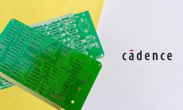
6.Design Cadence DEMO :
Cadence is a well-known provider of electronic design automation (EDA) software, including tools for PCB (Printed Circuit Board) design. Cadence offers a range of PCB design tools under its "Allegro" product line, and you can typically obtain a demo or evaluation version of these tools for a limited period to explore their features. Keep in mind that the availability and features of the demo version may vary over time, so it's advisable to visit the Cadence website or contact their sales or support team for the most up-to-date information on obtaining a demo
After successful purchase, this item would be added to your courses.You can access your courses in the following ways :
 Launch your Graphy